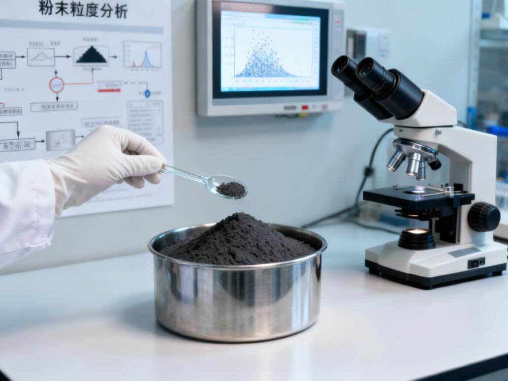
The probe card is used to test the function of the bare crystal with a probe before the chip is packaged. It is the interface between the tested chip (Chip) and the testing machine. It is a step that has a significant impact on the manufacturing cost in wafer testing. The yield of the finished product tested by the probe card can be increased by nearly 20%.
According to the VLSI report, the global probe card market is worth US $1.65 billion in 2018 and will reach more than US $2 billion in 2024, with an annual growth rate of more than 4%. The growth of the semiconductor industry as a whole has led to an increase in the use of probe cards for packaging testing, of which advanced probe cards (Advanced Probe Cards) is the main driving force for growth.
Moore's Law predicts that the number of transistors doubles every 24 months, which also means that the size of transistors needs to continue to shrink; this poses an increasingly stringent challenge to packaging testing requirements, thus stimulating the rapid development of innovative closed testing technologies such as advanced probe cards. Compared with the traditional probe card, the advanced probe card shows obvious changes: the increase of the number of probes, the reduction of probe size, the shortening of detection spacing, the increase of material thickness, the variety of holes and the continuous innovation of new materials, and so on. These trends pose great challenges to the production of probes and all the components that make up probe cards, among which the key guide plate manufacturing is a headache for traditional manufacturers.
The traditional mechanical drilling technology is often used to process the guide plate, but due to the limitation of the bit size, the hole diameter of the round hole is generally more than 40um, and the unilateral size of the special-shaped hole is more than 100um. The minimum spacing of this process is not less than 50um, and the processing time of a single hole is more than 10 seconds. In order to reduce the contact force (touchdown) and production cost in the advanced probe card, a new policy structure has been developed in recent years, which has led to a surge in demand for matching square hole guides. How to manufacture the square hole of 30-60um size has become the most serious obstacle for probe card enterprises to become one of the world's first-class manufacturers.
GF's mature laser micro-hole processing technology provides an efficient and high-quality solution for micro-square hole processing. The ultrafast laser we are equipped with has the characteristics of short pulse and high energy density, and there is no burn around the processing material, and there is no burr on the hole wall; the multi-function rotary cutting technology with galvanometer system avoids the positive cone hole that may be produced by traditional laser processing, and the processing of straight-through hole and even inverted cone hole is really realized.
We develop our own process for common materials in the probe card industry to maximize the processing efficiency of silicon nitride, alumina, zirconia and other materials. This allows our integrated solution to process square holes of 35 x 35um in 2 seconds with a fillet of only 3.5um and a spacing of 7um, and the heat-affected layer in the surrounding area is negligible.
In addition to showing a multiple increase in efficiency, the consistency and reliability of laser processing are also valued by our probe card users. Just imagine on a probe card with 10,000 square holes, if any kind of defect occurs in the final processing stage, it may lead to the scrapping of the whole probe card, and the loss of time and money cost is considerable. The following figure shows that after 24-hour continuous processing on the client side, the size difference between the entrance and outlet of the microhole is within ±1um, which records the stability requirements of the equipment in detail.