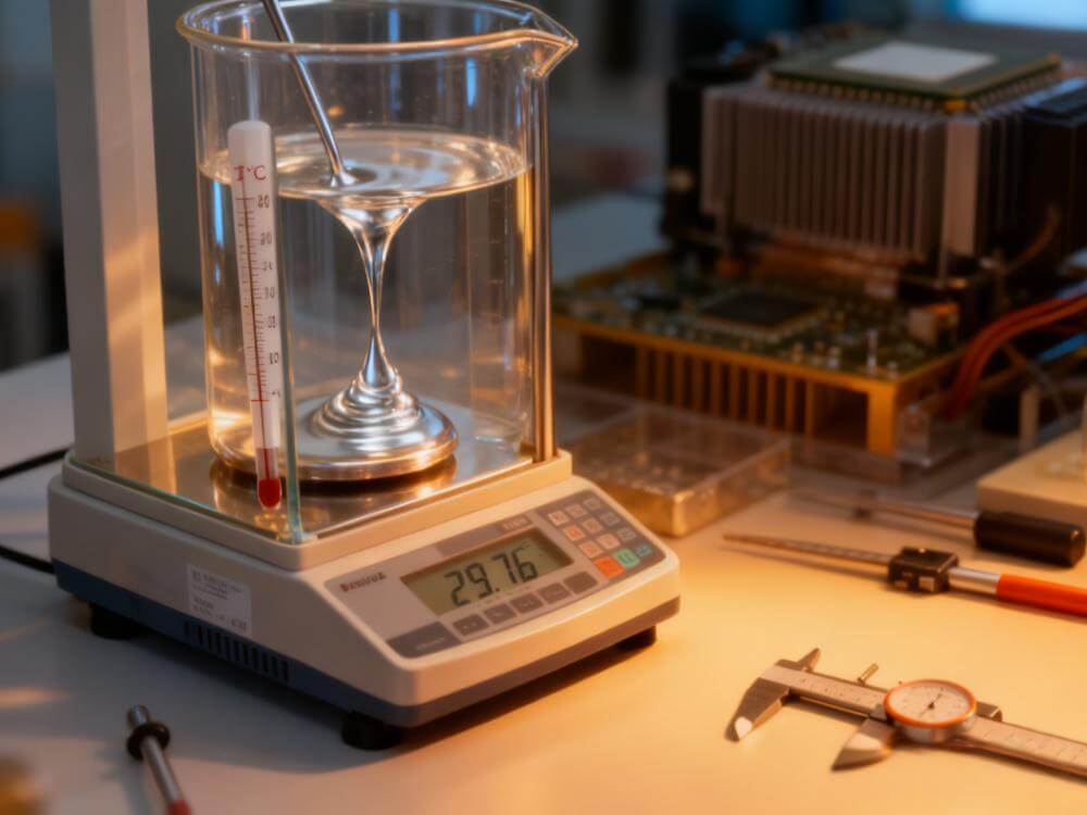
On May 6th, IBM released the world's first 2nm chip. The company said that the 2nm architecture chip can consume 75 per cent less power with the same performance as the existing 7nm, and that a mobile phone with the chip may only need to be recharged every four days. At the same time, it can also increase performance by 45 per cent at the same energy consumption as the existing 7nm. Compared with the most cutting-edge 5nm chips, 2nm chips are smaller and faster.
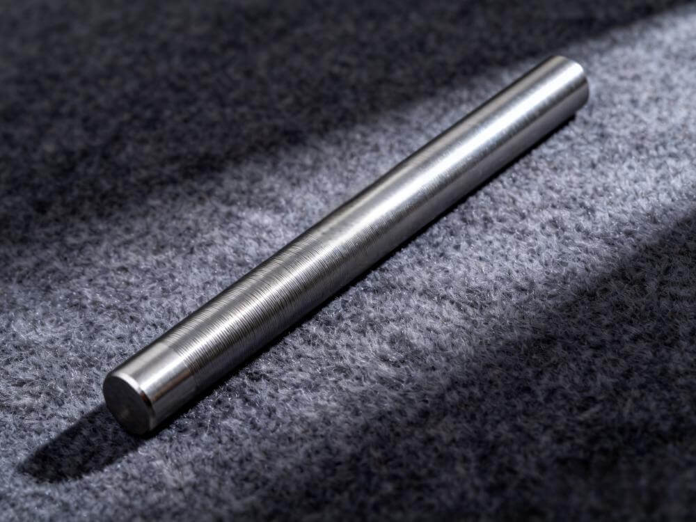
The key to this chip is to incorporate 50 billion transistors into a 150mm square chip.
IBM, once a major chipmaker, has outsourced much of its chip production to Samsung Electronics. But (Albany) still maintains a chip manufacturing R & D center in Albany, New York, where the world's first 2nm chip manufactured by IBM is coming from. The center is responsible for commissioning the chips and has signed joint technology development agreements with Samsung and Intel to use IBM's chip manufacturing technology.
However, even with the "must-kill" of 2nm chip manufacturing technology, IBM may not be able to shake off competitors such as TSMC, and the future depends on the mass production capacity of this new product.
Chip size is not the only criterion for judging performance in 3D era
In the era of 2D packaging, size is an effective measure of the advanced degree of the chip. However, with the advent of 3D transistors such as FinFET, it makes more sense to hold how many transistors per unit area.
Ian Cutress, a columnist for AnandTech, said in a commentary on May 6th that IBM claimed to have created the world's first 2nm chip, greatly boosting current chip production technology. However, at present, the so-called several nm has long been due to the development of chips from 2D plane to 3D. In the past, the meaning of comparing the minimum size of zero components has been lost, and it is more just a concept of "replacement". A more meaningful benchmark may be the number of transistors per unit area.
IBM's 2nm process claims to hold 50 billion transistors in an area of 150mm, with an average of 330 million transistors per square millimeter, and there are currently no comparable chips.
TSMC and Samsung's 7nm process is about 90 million transistors per square millimeter, Samsung's 5LPE is 130 million transistors, and TSMC's 5nm is 170 million transistors.
Comparison of transistor unit density among IBM, TSMC, Intel and Samsung chips of different sizes
Successful trial production and mass production are two different things.
IBM announced the success of the pilot 7nm process in 2015, but it was not until last August that the first commercial product, Power10 chip, appeared.
As a result, Ian Cutress said that the message of IBM is relatively strong, when there will be a product launch is another matter.
IBM withdrew from its contract manufacturing business as early as 2014 and sold its IBM Microelectronics department to GE Core, and its 2nm chip OEM business may be entrusted to AMD, Samsung, GE Core and Intel.
In addition, from the Power roadmap, IBM's most advanced Power10 chip is the 7nm process. Considering the conservatism of IBM's Power and z server business (the processor is being updated for three years), it seems that there is no need to use 2nm technology when the Power11 in the design and the Power12 in the whiteboard have 5nm and 3nm nodes to use.
Previously, Mukesh Khare, the core research and development staff of IBM semiconductors, also predicted that the newer generation of Power11 should appear around 2023, using mature 5nm process.
It is worth noting that competitors are in hot pursuit. At present, among the process technologies that can be mass produced, TSMC 5nm technology takes the lead, which is used in Apple's M1 and A14 chips and Huawei's Kirin 9000, followed by Samsung's 5LPE process, used in Qualcomm Snapdragon 888 chips.
The exploration of advanced processes continues. TSMC's 4nm and 3nm chips are expected to be mass produced next year, and 2nm chips have also made a key breakthrough, keeping pace with IBM. Intel's 7nm process chip is expected to go into production in 2023.