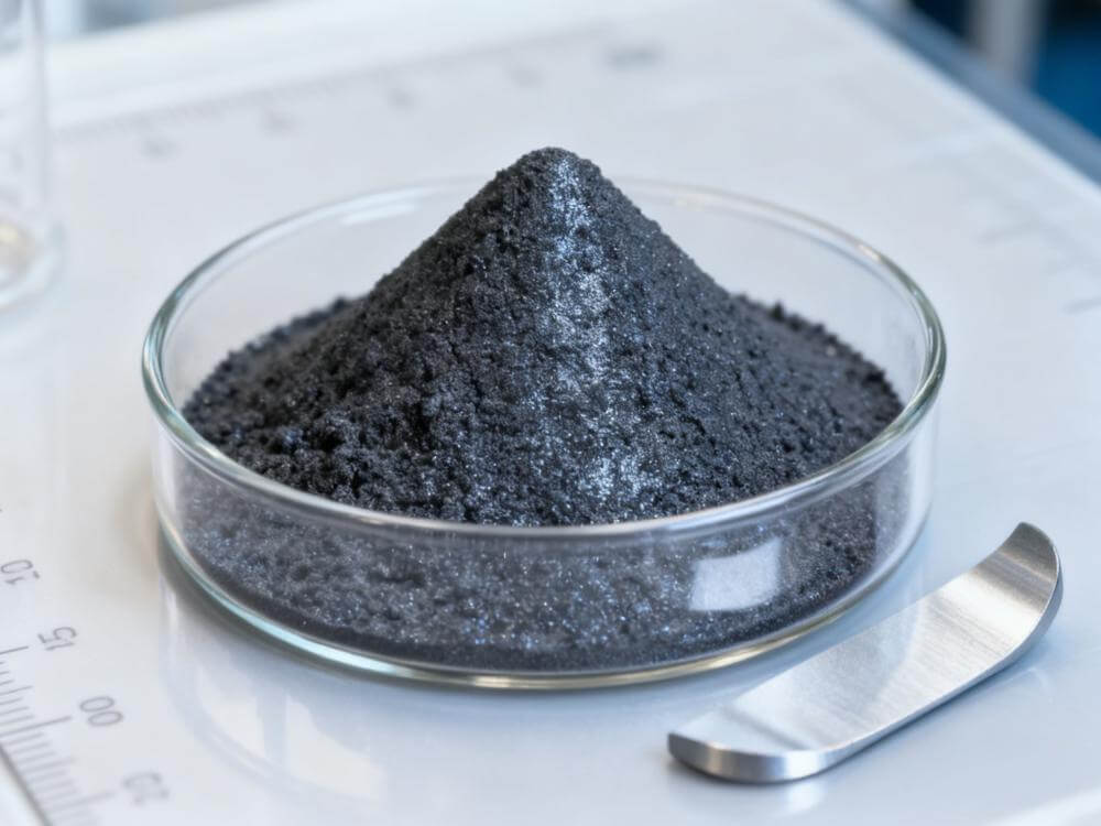

Zhejiang Zhonghe Science and Technology Co., Ltd. (hereinafter referred to as: Zhonghe Technology) announced that the company's holding subsidiary Zhejiang Hainer Semiconductor Co., Ltd. (hereinafter referred to as: Zhejiang Hainer) plans to invest no more than 520 million yuan to build a domestic semiconductor medium and large size single crystal base project to accelerate the layout of medium and large size silicon single crystal products market.
The announcement shows that the project will rely on Zhejiang Hainer's own professional team and external cooperation experts, using free technology or the introduction of overseas (Japan) advanced crystal technology, to build a production base with an annual output of 750 tons of 6-to 8-inch semiconductor-level monocrystalline silicon (including lightly doped and heavily doped single crystals), and to complete the research and development of related production technologies of 12-inch semiconductor-level monocrystalline silicon. The construction of this project will help Zhejiang Haina to break through the business ceiling of 4-to 6-inch products at the present stage, which is in line with the overall development plan of "Pan-Semiconductor Wings" in the company's "one body and two wings" and in line with the chip material localization strategy.
According to Zhonghe Technology, Zhejiang Hainer is the core business body of the company's pan-semiconductor business plate, and the above projects are built to solve the problem of insufficient single crystal production capacity, promote the optimization and upgrading of products such as overall semiconductor silicon wafers and improve their quality. to meet the increasingly prominent localization needs of medium and large-sized semiconductor wafers in China, and to comply with the large-size and functional industry development trend of the semiconductor wafer industry, to improve efficiency and reduce costs.
In addition, in order to ensure the orderly implementation of the single crystal base project, Zhejiang Hainer plans to set up a new wholly-owned subsidiary in Shanxi Province as the main body of operation and construction, with a registered capital of no more than 150 million yuan. The company name is Heiner Semiconductor (Shanxi) Co., Ltd. (subject to industrial and commercial registration).
![[속보 | 칠레 광업생산지수, 7월 전년 대비 7.2% 하락… 금속광업 10.7% 감소]](https://imgqn.smm.cn/usercenter/bFzkj20251217171724.jpg)
![[SMM 크로뮴 플래시] 짐바브웨, 광물 밀수 단속으로 크롬 정광 1,500톤 비축분 압류](https://imgqn.smm.cn/usercenter/pAOxy20251217171725.jpg)
![[SMM 크롬 플래시] 미국 강제노동 관세, 섹션 232 면제 없이 남아공 페로크롬에 타격](https://imgqn.smm.cn/usercenter/cgspx20251217171725.jpg)