

[Applied Materials выпускает серию оборудования для 3D-производства ИИ-чипов, ориентированного на процесс стековой сборки HBM]
Заявление об источниках данных: За исключением общедоступной информации, все остальные данные обрабатываются SMM на основе общедоступной информации, рыночного общения и с опорой на внутреннюю базу данных и модели SMM. Они приведены только для справки и не являются рекомендациями для принятия решений.
По любым вопросам или для получения дополнительной информации, пожалуйста, свяжитесь: lemonzhao@smm.cn
Для получения дополнительной информации о доступе к нашим исследовательским отчётам обращайтесь:service.en@smm.cn
Связанные новости
![Доллар слабеет, цветные металлы демонстрируют смешанную динамику; никель на LME и SHFE, серебро на SHFE выросли более чем на 1%, коксующийся уголь и кокс упали более чем на 2% [Ночной рынок]](https://imgqn.smm.cn/usercenter/qopTu20251217171736.jpg)
15 минут назад
Доллар слабеет, цветные металлы демонстрируют смешанную динамику; никель на LME и SHFE, серебро на SHFE выросли более чем на 1%, коксующийся уголь и кокс упали более чем на 2% [Ночной рынок]
Читать далее
Доллар слабеет, цветные металлы демонстрируют смешанную динамику; никель на LME и SHFE, серебро на SHFE выросли более чем на 1%, коксующийся уголь и кокс упали более чем на 2% [Ночной рынок]
15 минут назад
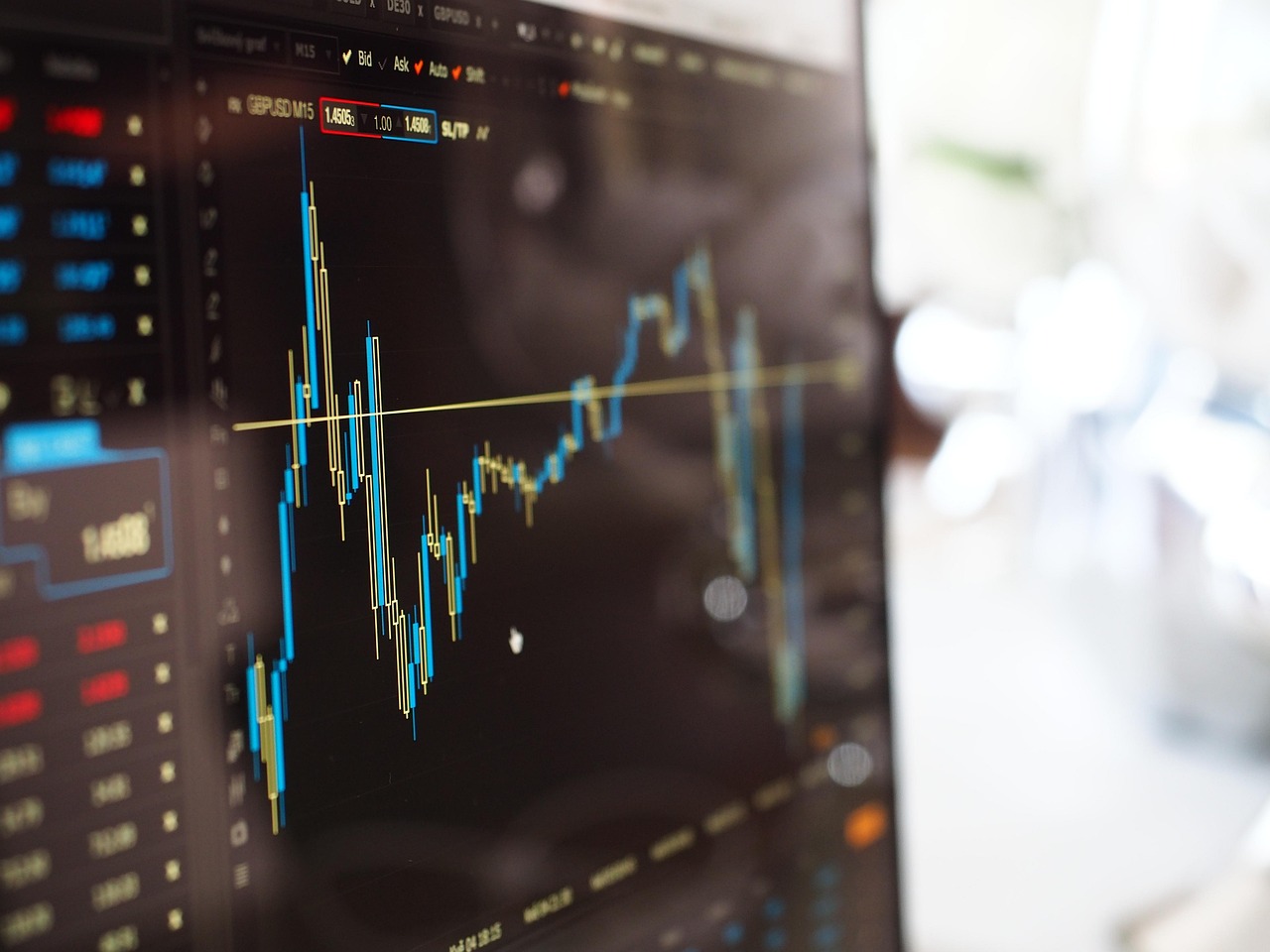
15 часов назад
Ваши клиенты ищут вас! Более 1000 лиц, принимающих решения в отраслевой цепочке, соберутся в Исине
Читать далее
Ваши клиенты ищут вас! Более 1000 лиц, принимающих решения в отраслевой цепочке, соберутся в Исине
15 часов назад
![Шанхайская биржа цветных металлов: цены на алюминий слегка выросли, темпы восстановления замедлились; на рынке глинозема наблюдается избыток предложения и слабый спрос, что ограничивает потенциал роста [Краткий обзор SMM по алюминию]](https://imgqn.smm.cn/usercenter/NQyKF20251217171655.jpg)
17 часов назад
Шанхайская биржа цветных металлов: цены на алюминий слегка выросли, темпы восстановления замедлились; на рынке глинозема наблюдается избыток предложения и слабый спрос, что ограничивает потенциал роста [Краткий обзор SMM по алюминию]
Читать далее
Шанхайская биржа цветных металлов: цены на алюминий слегка выросли, темпы восстановления замедлились; на рынке глинозема наблюдается избыток предложения и слабый спрос, что ограничивает потенциал роста [Краткий обзор SMM по алюминию]
17 часов назад
Связанные новости
Доллар слабеет, цветные металлы демонстрируют смешанную динамику; никель на LME и SHFE, серебро на SHFE выросли более чем на 1%, коксующийся уголь и кокс упали более чем на 2% [Ночной рынок]
Sep 03, 2026 08:33
Ваши клиенты ищут вас! Более 1000 лиц, принимающих решения в отраслевой цепочке, соберутся в Исине
Sep 02, 2026 16:52
Шанхайская биржа цветных металлов: цены на алюминий слегка выросли, темпы восстановления замедлились; на рынке глинозема наблюдается избыток предложения и слабый спрос, что ограничивает потенциал роста [Краткий обзор SMM по алюминию]
Sep 02, 2026 15:34
Августовский коэффициент использования мощностей в производстве медной проволоки и кабеля немного вырос; качество восстановления спроса ещё предстоит оценить [Анализ SMM]
Sep 02, 2026 14:59