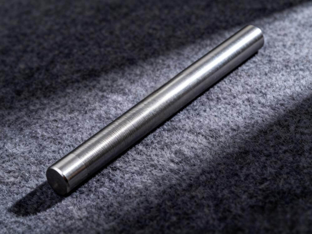
On June 2, Luxiao Technology said on the interactive platform recently: "after years of painstaking efforts, the company has made a breakthrough in the technology of the third generation semiconductor silicon carbide, a subversive material, and the equipment has been installed and debugged."
According to people in the industry told me: "the main product of Luxiao Technology is 6-inch conductive silicon carbide substrate, and the equipment has been installed and debugged, which means that the laboratory has already successfully made a sample, and Synchronize should carry out client-side verification. Who else would the product be made and sold to? At present, the best landing application of conductive silicon carbide should be in the field of automotive power semiconductors. in the news circle, it is rumored that Luxiao Technology has had substantial contact with the process leader of a domestic automobile company, and it is very likely that it has begun to do product verification. if this news is true, then Luxiao is indeed the only company in A-share listed companies that can really come up with physical objects at present. Indeed, in the past two days, a picture has circulated in the circle that looks like a laughing silicon carbide wafer. Most of the silicon carbide substrate manufacturing projects of other companies are planned in advance. I wonder if anyone has seen the silicon carbide wafer samples of other companies. "
It is understood that silicon carbide is a third generation semiconductor material, also known as wide band gap semiconductor material. The band gap width of silicon carbide is 3 times that of silicon, the thermal conductivity is 4-5 times that of Si, the breakdown voltage is 8 times that of Si, and the electron saturation drift rate is 2 times that of Si.
In other words, silicon carbide is especially suitable for manufacturing high-voltage and high-power chips. compared with the same type of silicon chips, silicon carbide has higher voltage resistance, greater resistance to high current, more resistance to high temperature, and the power chip has smaller size and higher reliability. there will be broad prospects in power semiconductors, especially in the field of automotive electronics in the future.
At present, silicon carbide MOSFET is used to replace the traditional silicon-based IGBT, in electric vehicles. For example, the Tesla Model 3 model uses the silicon carbide single tube of Infineon and Italian semiconductors.
There are two types of silicon carbide substrates, semi-insulating and conductive. The semi-insulating type is mainly used to produce high-power RF devices, such as silicon carbide-based gallium nitride power amplifier for 5G base stations, while the conductive type is used to produce silicon carbide high-voltage high-power devices mentioned above, such as silicon carbide MOSFET used in electric vehicles.
Although the prospect of silicon carbide is huge, it is very difficult to make silicon carbide crystals and substrates at present, according to a person in the industry. The common silicon material can grow about 2 meters crystal in 72 hours, but the silicon carbide crystal thickness is only 2-3 centimeters in 144 hours. The growth rate of silicon carbide is less than 1% of that of silicon.
Secondly, silicon carbide is very hard. Its Mohs hardness is as high as 9.5, second only to 9.9 diamond, and it is one of the hardest objects in the world. Therefore, the follow-up processing of cutting, grinding and polishing is much more difficult than silicon material. According to the professional, the cutting efficiency of silicon carbide is very slow at present. A 3 cm thick ingot can cut about 35-40 pieces, but it takes nearly 120 hours. It takes five days, which is much slower than cutting silicon ingots.
Therefore, it is very difficult to make a complete silicon carbide substrate, and the price is very high. However, due to the strong performance advantages of silicon carbide, the demand for silicon carbide substrate materials from downstream customers is extremely strong, coupled with the further demand for silicon carbide wafers from automotive electronics, which makes it "difficult to obtain" silicon carbide at present. Sources revealed that at present, the international giant CREE of the United States monopolizes 70% of the production capacity of silicon carbide, and the production capacity within 5 years is bound by the long Association orders of Italian Semiconductor, Infineon, Roma and other companies.
Although there are Shandong Tianyue, Tianke and other silicon carbide substrate manufacturing enterprises in China, most of the products are semi-insulating substrates for RF, not conductive substrates for power chips, and mainly with a size of 4 inches. Assuming that Luxiao's 6-inch conductive silicon carbide wafer can be successfully mass-produced, it not only fills the domestic gap, but also has a leading position in the competition.
At present, the industry is still actively exploring the technology of efficient silicon carbide crystal growth and cutting and polishing, but at present, it is difficult to break through the difficulties in the short term, and it is difficult to improve the efficiency significantly. Therefore, whoever has more production equipment and who expands production quickly will be in a dominant position in the competition. And now the downstream customer demand is strong, as long as the product quality passes, and can maintain a stable supply, there is no shortage of orders at all, and the future opportunity is very great.