SMM9 March 3: some time ago, the Dutch ASML lithography machine import has become the focus of the public, but the chip is a high degree of crystallization of human wisdom, there are many other complex steps in the production process in addition to lithography. A wafer is a silicon wafer used in the fabrication of silicon semiconductor integrated circuits, and its original material is silicon. High purity polysilicon is dissolved and mixed with silicon crystal seed to form cylindrical monocrystalline silicon. After grinding, polishing and slicing, the silicon wafer is formed, that is, the wafer. At present, the domestic wafer production lines are mainly 8 inches and 12 inches. On the silicon wafer, it can be processed into a variety of circuit element structures, and become IC products with specific electrical functions.
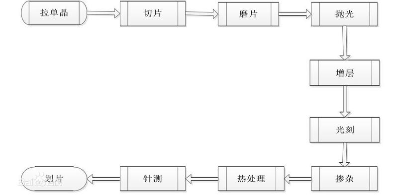
Manufacturing process
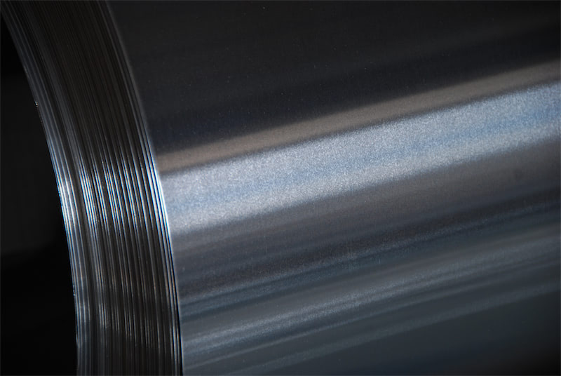
The original material of the wafer is silicon, and there is an inexhaustible amount of silicon dioxide on the surface of the earth's crust. The silicon dioxide ore is extracted by electric arc furnace, chlorinated with hydrochloric acid, and distilled to produce high-purity polysilicon with a purity of 99.999999999%. The main processing methods of wafers are wafer processing and batch processing, that is, one or more wafers are processed at the same time. With the smaller and smaller feature size of semiconductors and more and more advanced processing and measuring equipment, new data features have emerged in wafer processing. At the same time, with the decrease of the feature size, the influence of the number of particles in the air on the quality and reliability of the wafer increases, and with the improvement of cleanliness, the number of particles also appears new data features.
Deoxidizing and purifying sand and quartz are deoxidized and purified to obtain Si02 silica with a silicon content of 25%. Silicon oxide is extracted by electric arc furnace, chlorinated with hydrochloric acid, and distilled to obtain crystalline silicon with a purity of more than 99%.
The crystal silicon is molded at high temperature and the round crystal rod is made by rotating and stretching.
Wafer slicing cuts the wafer transversely into wafers with basically the same thickness, Wafer.
Wafer polishing, grinding and polishing the appearance of the wafer.
Wafer coating produces a layer of Si02 silicon dioxide on the wafer at high temperature or in other ways. Si02 silica is an insulating material, but Si02 silica with impurities and special treatment has certain electrical conductivity. Here the function of Si02 silica is for the conduction of light, which is for subsequent lithography.
Photoresist photoresist is the same as previous photographic film. Wafer photoresist is required to be thin and smooth.
Lithography (extreme Violet Lithography EVO) the designed wafer circuit mask is placed under the ultraviolet radiation of the lithography, and then the Wafer is placed under the wafer mask. At the moment of lithography, the photoresist in the part of the Wafer that was etched melts and is engraved with a circuit diagram. To remove the photoresist, the pattern on the photoresist should be consistent with that on the mask. Lithography again. The circuit of a wafer undergoes multiple lithography. With the advent of the new technology of extreme purple lithography, the lithography of wafers has become more accurate and efficient, and can even be completed all at once.
Ion injection is injected into the wafer circuit of photolithography by ion injection in a vacuum. It is usually injected with ions after a lithography.
Electroplating A layer of copper sulfate on a wafer. Copper ions go from positive to negative.
Polishing and polishing the surface of Wafer, the whole Wafer has been manufactured successfully.
The wafer slice cuts the Wafer into a single wafer Die.
Testing is mainly divided into three categories: functional testing, performance testing, anti-aging testing. Such as: contact testing, power consumption testing, input leakage testing, output level testing, dynamic parameter testing, analog signal parameter testing and so on. If there is a bad wafer, it will be scrapped, and this is black film; some of the wafers that have failed the test but do not affect the use of the wafer will be divided into white film, which can flow out; and all those that have passed the test will be positive film. After the calculation, the next step is packed into the box and sent to the closed test, Die (naked chip.) after the closed test, it has become the chip on our electronic digital products.
Common Wafer Manufacturing process of 200mm CMOS Chip
Wafer specification
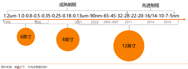
At present, there are three specifications for using the most mainstream wafers in the global chip market: 6-inch, 8-inch and 12-inch. At present, 12-inch wafers are the mainstream in the market, and nearly 70% of the production capacity is 12-inch wafers. The larger the size of the wafer, the more difficult it is to make, and of course, the more chips these big wafers cut out. At present, 12-inch wafers are the mainstream in the market, and nearly 70% of the production capacity is 12-inch wafers.
Generally speaking, different kinds of chips use different wafer specifications, and the trend of wafer specifications is becoming larger and larger on the whole.
Power semiconductors-6-inch and 8-inch wafers
Processors such as MCU-8-inch wafers
Logic chips and memory chips-- 12-inch wafers
From the point of view of the field of use, the strongest demand for 12-inch wafers is the memory chips (NAND and DRAM), 8-inch wafers are more used in automotive electronics and other fields.
In addition, the process of different sizes of wafers is often different. According to the type of process, wafer can be divided into three types: polished wafer, epitaxial wafer and SOI wafer.
Generally speaking, polished wafers are used for integrated circuit production lines less than 8 inches, and epitaxial wafers are used for 45nm and 12-inch wafers with line width below. SOI is a new process. Polishing wafer is the most widely used process, because other processes are developed on the basis of polishing wafer, and polishing wafer can be used to make substrate materials for memory chips, power devices and epitaxial wafers.
Epitaxial wafers grow a layer of monocrystalline silicon on the basis of polished wafers, which are generally used in the manufacture of general-purpose processor chips, diodes and IGBT power devices.
SOI is mainly used in RF front-end chips, power devices, automotive electronics and other fields.
Wafer capacity
Since 2000, the semiconductor industry has increased chip shipments by increasing the number of wafers, and the use of process miniaturization to cut more chips per wafer has not contributed much. From 2000 to 2019, the average annual growth rate of quality chips cut from each wafer was only 0.9%, but the average annual growth rate of quality chips increased by increasing wafer casting reached 6.5%. Overall, 86% of the annual increase in the number of chips in the world from 2000 to 2019 comes from the increase in the number of wafers, and only 14% comes from the process miniaturization that allows each wafer to cut more chips. Therefore, wafer capacity means potential sales, which is a major factor affecting manufacturers' revenue.
From the analysis of supply and demand structure, the global production capacity of supply-side 2019Q4 wafers, 200mm has dropped to 5 million wafers / month, at the same level as when the 2016 cycle started, 300mm is close to 6 million wafers / month, falling below the high water level of the boom, considering the existence of a high-performance computing chip / fingerprint recognition die area increase; 2 new applications (5G/ vehicle networking / cloud computing) and other required silicon content has increased, a tight balance between supply and demand has emerged.
Wafer industry chain
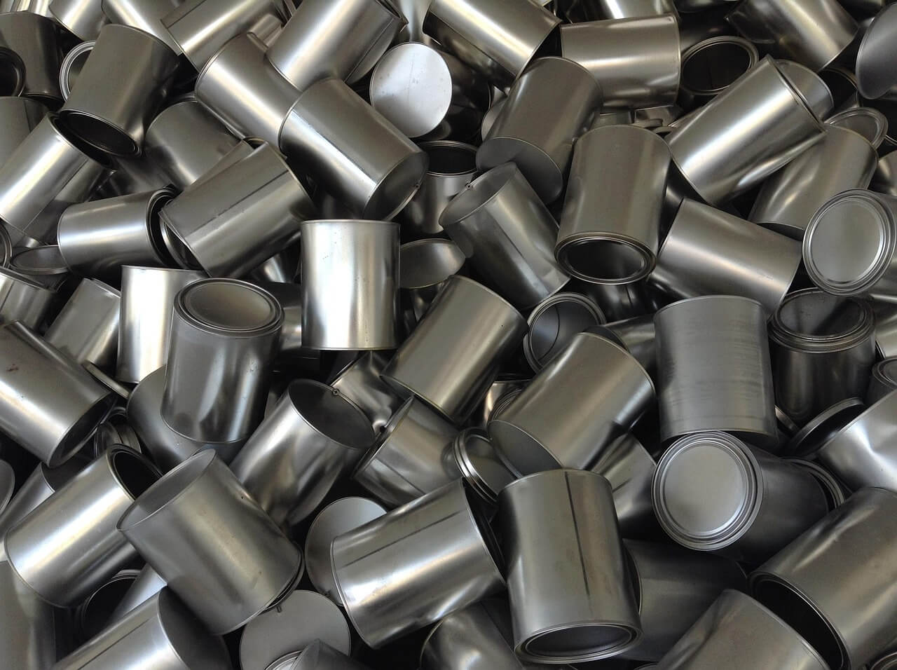
At present, the wafer market on the market is basically monopolized by about 15 wafer factories with a 95% share, mainly because it is very difficult to manufacture wafers, and customers have very high requirements for purity and size. Domestic wafer factories are facing a situation of breaking through adversity. The upstream chip manufacturing closed test support industry is mainly semiconductor equipment and material providers; the middle semiconductor manufacturing industry is divided into three parts: integrated circuit design, manufacturing and closed testing. IC designers include Huawei, Qualcomm, AMD and Nvidia. Downstream semiconductor terminal applications include automotive electronics, industrial electronics, communications, consumer electronics, PC and other fields.
On the supply side, silicon wafer factory produces single crystal silicon wafer, which is the upstream of chip foundry. Silicon wafer is the most commonly used semiconductor material and the material with the highest cost in the process of chip production.
According to Citic Securities data, from the silicon wafer supplier pattern: Japanese factory control, oligopoly pattern is stable. Japanese manufacturers account for more than 50% of the market share of silicon wafers. The top five manufacturers account for more than 90% of the world. Among them, Japan Shinyue Chemical accounts for 27%, Japan SUMCO accounts for 26%, and the two Japanese manufacturers have a combined share of 53%, more than half. Taiwan Global Wafer of China acquired SunEdison Semiconductor of the United States during the trough of the wafer industry in December 2016, rising from the sixth to the third, accounting for 17%, Germany's Siltronic accounted for 13%, and South Korea's SK Siltron (was acquired by SK Group in 2017) accounted for 9%, which is different from the top four manufacturers. SK Siltron only supplies Korean customers.
At present, the enterprises with silicon wafer production capacity in China mainly include Zhejiang Jin Ruihong, Beijing Research Institute and Shanghai Xinyi. China has Central shares, as well as Shanghai Xinyang shares in the production of companies.
In addition, there are French Soitec, Taiwan Taisheng, Hejing, Jiajing and other enterprises, the share is relatively small. The types and sizes of wafers supplied by each major manufacturer are different, and generally speaking, the products of the top three manufacturers are more diverse. The top three manufacturers can supply Si annealed wafers and SOI wafers, of which only Nippon Shinyue can supply 12-inch SOI wafers. German Siltronic and Korean SK Siltron do not provide SOI wafer, SK Siltron does not supply Si annealed wafer. However, there is basically no difference in size between Si polished wafer and Si epitaxial wafer.
The demand side is mainly IC design and production manufacturers, chip manufacturers are called wafer factories. Giants have high barriers to competition, and AI chips have become a new driving force for growth since 2018. Qualcomm, Broadcom, MediaTek, Apple and other manufacturers are the strongest, while mainland manufacturers Hays are on the rise. With the development of science and technology leading the upgrading of terminal products, innovative applications such as AI chips have an increasing demand for IC products. It is estimated that by 2020, the market size of AI chips will rise from about US $600 million in 2016 to US $2.6 billion, with CAGR reaching 43.9%. At present, domestic and foreign IC designers are actively laying out the AI chip industry. Nvidia is the market leader in AI chips, and AMD and Tesla are jointly developing AI chips for autopilot.
For domestic manufacturers, Hayes, Zhan Rui and other mobile processing chip and baseband chip manufacturers rely on the rapid rise of China's smartphone market in recent years, becoming one of the top ten IC designs in the world. Heath chips have been fully applied to Huawei smartphones, and Samsung, Xiaomi and other manufacturers have also adopted self-developed chips. now China is the world's largest terminal demand market, so the domestic IC design industry has a huge development advantage.
In terms of IC design, giants control high barriers to competition, and AI chips have become a new driving force for growth since 2018. Qualcomm, Broadcom, MediaTek, Apple and other manufacturers are the strongest, while mainland manufacturers Hayes are on the rise. With the development of science and technology leading the upgrading of terminal products, innovative applications such as AI chips have an increasing demand for IC products. It is estimated that by 2020, the market size of AI chips will rise from about US $600 million in 2016 to US $2.6 billion, with CAGR reaching 43.9%. At present, domestic and foreign IC designers are actively laying out the AI chip industry. Nvidia is the market leader in AI chips, and AMD and Tesla are jointly developing AI chips for autopilot.
The growth rate of China's silicon wafer market leads the world. With the advent of the peak of wafer production in China, the semiconductor wafer market in mainland China has entered a stage of rapid development. From 2016 to 2018, semiconductor wafer sales in mainland China rose from US $500m to US $1 billion, with an average annual compound growth rate of 40.8 per cent, much higher than the global market in the same period.
Terminal application
Smartphone, PC
Smart phone core chips involve advanced processes and compound semiconductor materials. In order to meet the needs of high-performance computing and long-range heat dissipation, CPU has an increasing demand for chip processes. Mobile phones and computers are the first to adopt advanced processes. In terms of performance, according to techcenturion evaluation, the best performance of the mobile phone CPU chip is Apple's A13, which uses TSMC's 7nm process.
Communication base station
Communication base stations are highly dependent on foreign chips, and they are mainly American chip enterprises. At present, the base station system is mainly composed of baseband processing unit (BBU) and radio frequency pull unit (RRU). Usually one BBU corresponds to multiple RRU devices. The main difficulty is that RRU chip devices involve high-power RF scenarios, usually using gallium arsenide or gallium nitride materials.
Automotive electronics
Automotive electronics demand for semiconductor devices are mainly MCU, NOR Flash, IGBT and so on. The internal demand of traditional automobile is mainly MCU, including power control, safety control, engine control, chassis control, vehicle electrical appliances and so on. The new energy vehicle also includes electronic control unit ECU, power control unit PCU, electric vehicle control unit VCU, hybrid vehicle controller HCU, battery management system BMS and inverter core components IGBT.
AI and Mining Machine Chip 5G, IoT
AI chip and miner chip belong to high-performance computing, which requires higher advanced process. In the AI and blockchain scenarios, the traditional CPU has insufficient computing power, and the new architecture chip has become a development trend. At present, there are mainly chip paths that continue the traditional architecture, such as GPU, FPGA, ASIC (TPU, NPU, etc., and the chip path that completely subverts the traditional computing architecture and uses the structure of simulated human brain neurons to improve computing power. GPU is ecologically leading in the cloud, and terminal scenario specialization is the future trend.
The field of 5G radiation can be further subdivided into telecom base station equipment, smart phone / tablet computer, networked vehicles, networked equipment, broadband access gateway equipment and so on. According to Grand View Research, the smartphone / tablet segment is estimated to reach $627.07 million by 2019. Games, UHD video and video calls drive demand for 5G smartphones. In addition, continued investment in the deployment of 5G telecommunications network infrastructure has increased the overall demand for 5G chipset components. The global 5G chipset market is estimated to grow at a compound annual growth rate of 69.7% from 2020 to 2025.
Click to understand and sign up for the 2020 China Automotive New Materials Application Summit Forum.
Scan the QR code above to view the business cards of the participating companies and sign up online

Scan the code and apply to join the SMM Automotive Industry Exchange Group.