Shengmei Semiconductor equipment (Shanghai) Co., Ltd. (hereinafter referred to as Shengmei Shanghai) (Science and Technology Innovation Board Stock Code: 688082), a leading provider of wafer process solutions for semiconductor foreground and advanced wafer-level packaging (WLP) applications, has launched a series of integrated equipment to support compound semiconductor manufacturing. The company's 150mm compatible system extends the wet series of front integrated circuits and advanced wafer level packaging to support applications in the field of compound semiconductors, including gallium nitride (GaAs), gallium nitride (GaN) and silicon carbide (SiC) processes. The compound semiconductor wet process product line includes gluing equipment, development equipment, photoresist de-gluing equipment, wet etching equipment, cleaning equipment and metal plating equipment, and is automatically compatible with flat edges or notched wafers.
Products meet the growing needs of electric vehicles, 5G communications, radio frequency and artificial intelligence markets.
"with the growth of demand in different markets, the compound semiconductor industry is developing rapidly." Dr. Wang Hui, chairman of Shengmei Shanghai, said, "through the investigation of this industry, we realize that we should make use of the important expertise and technology in the existing wet process products of front-road integrated circuits and advanced wafer-level packaging. To provide cost-effective and high-performance products that meet the technical requirements of compound semiconductors. We believe that the compound semiconductor equipment market provides an important growth opportunity for Shengmei Shanghai, as GaAs, GaN and SiC devices are becoming an increasingly integral part of future electric vehicles, 5G communications systems and artificial intelligence solutions. "
Shengmei Shanghai compound Semiconductor equipment Series
Ultra C silicon carbide cleaning equipment
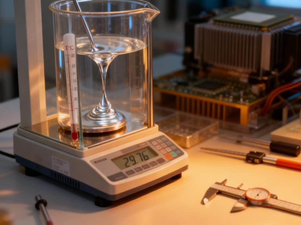
Ultra C silicon carbide cleaning equipment in Shengmei Shanghai uses sulfuric acid shuang oxygen water mixture (SPM) for surface oxidation and hydrofluoric acid (HF) to remove residues and clean silicon carbide wafers. The equipment also integrates Shengmei Shanghai's SAPS and Megasonix cleaning technology to achieve more comprehensive and deeper cleaning. Ultra C silicon carbide cleaning equipment provides industry-leading cleanliness of ≤ 10ea0.3um per wafer and metal content < 1E10atoms/cm3 level. The device can clean more than 70 wafers per hour and will be available in the second half of 2022.
Ultra C wet etching equipment
It can provide < 2% uniformity, < 10% coplanarity and < 3% repeatability for gallium and indium gallium phosphide (InGaP) process. Ultra C wet etching equipment provides industry-leading chemical temperature control and etching uniformity. The equipment will be delivered to and tested by an important customer in the third quarter of 2022.
Ultra ECP GIII 1309 Applianc
Shengmei Shanghai's Ultra ECP GIII 1309 equipment integrates pre-wetting and post-cleaning cavities to support copper columns and solders for copper, nickel and tin-silver, as well as redistribution layer (RDL) and under-bump metallization (UBM) processes. The device achieves a uniformity of less than 3% and a repetition of less than 2% in the wafer and mold. The equipment was delivered to the customer in mid-2021 and meets the customer's technical requirements.
Ultra ECP GIII 1108 Applianc
The Ultra ECP GIII 1108 equipment provides gold bump, film and deep through hole processes that integrate pre-wetting and post-cleaning cavities. The equipment uses Shengmei Shanghai's tried-and-tested grid plate technology for deep-hole electroplating to improve ladder coverage. It can achieve a uniformity of < 3% and a repetition of < 2% in the wafer and mold. The cavity and the process tank are specially designed to avoid the oxidation of the gold plating solution, and the process tank has the function of nitrogen purging, which can reduce the oxidation. The equipment was delivered to key customers at the end of last year.
Ultra C ct glue coating equipment
The Ultra C ct glue coating equipment in Shengmei Shanghai adopts secondary rotation glue coating technology, which can realize uniform glue coating. The equipment has industry-leading advantages, including accurate glue control, automatic cleaning, hot and cold plate modules and independent process control for each cavity.
Ultra C dv developing equipment
In the compound semiconductor process, Shengmei Shanghai's Ultra C dv development equipment can carry out the key steps of baking, development and hard baking after exposure. Using the advanced technology of Shengmei Shanghai, the equipment can realize the flow rate of + /-0.03C and the temperature control of + /-0.5C according to the requirements.
Ultra C s brushing equipment
Ultra C s brushing equipment is based on Shengmei Shanghai's advanced wet cleaning technology to achieve excellent pollutant removal efficiency. The equipment achieves high performance through nitrogen atomization two-fluid cleaning or high-pressure cleaning to clean small particles more effectively. In addition, the equipment is compatible with Shengmei Shanghai's proprietary mega-acoustic cleaning technology to ensure excellent particle removal efficiency (PRE), without damaging the fine graphic structure.
Ultra C pr wet degumming equipment
Shengmei Shanghai's Ultra C pr wet degumming equipment uses trough soaking and monolithic processes to ensure efficient compound semiconductor degumming. The equipment was recently ordered by (IDM), a leading global manufacturer of integrated components, to remove photoresist, further confirming the technological advantages of Shengmei Shanghai.
Ultra SFP stress-free polishing equipment
Ultra SFP provides an environmentally friendly alternative for traditional chemical mechanical polishing in silicon through-hole (TSV) process and fan-out wafer-level packaging (FOWLP) applications. In TSV applications, Shengmei Shanghai's stress-free polishing (SFP) system can significantly reduce consumables costs by using proprietary electropolishing technology to remove copper coatings as low as 0.2 μ m, then using traditional CMP to further remove the remaining copper to the barrier layer, and wet etching to remove the barrier layer. The same process for FOWLP, can overcome the wafer warping caused by the stress of thick copper layer, and can be applied to the copper coating in RDL and flattened.