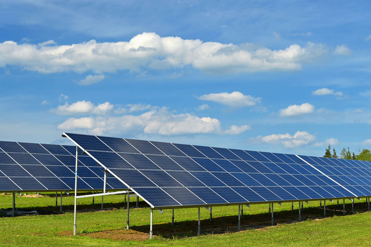
As the global solar photovoltaic (PV) industry continues to develop, PV modules have become a key link connecting upstream materials, solar cell manufacturing, and downstream PV systems. Although polysilicon, silicon wafers, solar cells, and PV modules belong to the same industrial value chain, they differ significantly in material form, manufacturing processes, and functions.
How is a PV module manufactured from upstream silicon materials? What is the difference between a silicon wafer and a solar cell? Why must solar cells undergo further encapsulation before becoming finished modules? What do common product specifications such as 48-format, 72-format, 18X, and 210R represent? And how are cell technologies such as PERC, TOPCon, HJT, and BC related?
These questions correspond to several key aspects of PV modules: upstream materials, module manufacturing, product specifications, and solar cell technology pathways. From a supply chain perspective, silica-bearing raw materials such as quartz undergo smelting and purification to produce metallurgical-grade silicon and polysilicon. These materials are subsequently processed into silicon wafers and solar cells. The cells are then electrically interconnected, encapsulated, and structurally assembled to form finished modules suitable for integration into PV systems.
Therefore, understanding a PV module begins with tracing its upstream supply chain, examining how silicon materials are transformed from mineral resources into photovoltaic devices capable of converting sunlight into electricity, and ultimately into complete PV modules.
I. From Quartz to PV Modules: How Is a Solar Module Manufactured?
From Mineral Resources to Electricity: Understanding the PV Supply Chain
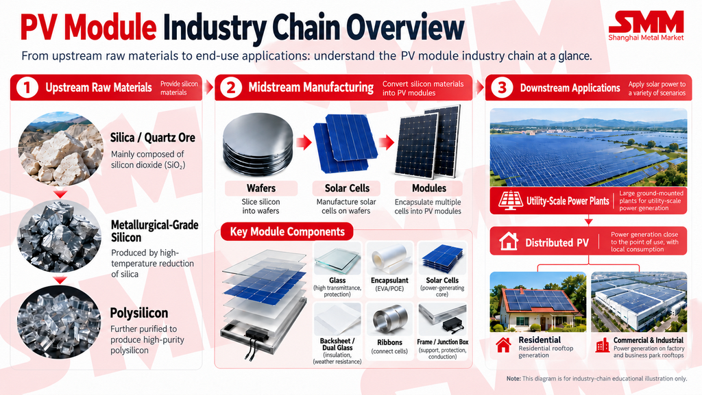
The upstream supply chain of PV modules can be traced back to silica-bearing mineral resources. Silicon materials undergo multiple processing stages, including metallurgical-grade silicon, polysilicon, silicon wafers, and solar cells, before being manufactured into PV modules and integrated into solar power systems.
The overall supply chain can be simplified as follows:
Quartz Raw Materials → Metallurgical-Grade Silicon → Polysilicon → Silicon Wafers → Solar Cells → PV Modules → PV Systems / Solar Power Plants
This supply chain can be understood as a progressive process involving silicon purification, material processing, and the development of photovoltaic functionality.
The initial stages primarily focus on material purity. Metallurgical-grade silicon is produced from naturally occurring silica-bearing materials and subsequently purified into high-purity polysilicon suitable for PV manufacturing. The purified silicon is then processed into wafers and further manufactured into solar cells capable of converting sunlight into electricity. At the module manufacturing stage, solar cells are combined with electrical interconnection materials, encapsulants, and structural components to produce PV products suitable for transportation, installation, and long-term operation.
From Quartz to High-Purity Polysilicon
One of the starting materials in the PV supply chain is quartz, which contains silicon dioxide (SiO₂). Quartz used in metallurgical-grade silicon production generally requires a relatively high SiO₂ content, typically reaching 99% or above, while certain high-grade raw materials may contain approximately 99.4%–99.8% SiO₂.
Natural quartz may also contain impurities such as iron, aluminum, calcium, and titanium. Consequently, the grade of the raw material, together with the types and concentrations of impurities, can directly influence subsequent smelting and purification processes.
An important distinction must first be made:
- The SiO₂ content of quartz is not equivalent to the purity of elemental silicon.
Silicon in quartz primarily exists in the form of silicon dioxide and must undergo high-temperature reduction before metallurgical-grade silicon can be obtained.
In a submerged arc furnace, quartz reacts with carbon-based reducing agents through high-temperature carbothermal reduction. The reaction can be represented in simplified form as:
SiO₂ + C → Si + CO₂↑
The resulting product is metallurgical-grade silicon, also commonly referred to as silicon metal, with a typical silicon purity of approximately 98%–99%.
Although this level of purity is relatively high for conventional industrial materials, it is insufficient for solar cell manufacturing.
Solar cells are semiconductor devices, and even low concentrations of impurities such as boron, phosphorus, iron, aluminum, and other metallic elements may affect the electrical properties of silicon materials and the conversion efficiency of finished cells.
Therefore, metallurgical-grade silicon must undergo further chemical purification to produce solar-grade polysilicon.
One of the commonly used polysilicon production technologies is the modified Siemens process. This process involves converting metallurgical-grade silicon into silicon-containing compounds that can be further purified. Impurities are removed through processes such as distillation, followed by reduction and deposition to obtain high-purity polysilicon.
Solar-grade polysilicon can typically achieve purity levels of approximately 6N–9N, where:
- 6N = 99.9999%
- 9N = 99.9999999%
Specific impurity control requirements vary depending on production processes, product specifications, and downstream applications. As a result, the actual purity of polysilicon products may differ.
By comparison, electronic-grade silicon materials used in semiconductor applications such as integrated circuits and microchips generally require more stringent control over overall purity and specific impurities, including boron, phosphorus, and metallic elements. Their purity can typically reach approximately 9N–11N or even higher.
The progression from quartz to high-purity silicon materials can therefore be summarized as follows:
Quartz with approximately 99% or higher SiO₂ content → Metallurgical-Grade Silicon with 98%–99% purity → Solar-Grade Polysilicon with 6N–9N purity → Higher-Purity Electronic-Grade Silicon
It should be noted that the distinction between solar-grade and electronic-grade silicon is not determined solely by the number of nines in their purity levels. The two categories also differ in requirements for specific impurities, material consistency, and production process control.
From Polysilicon to Electricity-Generating Solar Cells
High-purity polysilicon cannot generate electricity directly.
In the mainstream crystalline silicon PV industry, polysilicon is first processed through crystal growth to form monocrystalline silicon ingots. These ingots subsequently undergo squaring, slicing, and other processing steps to produce thin silicon wafers.
During crystal growth, specific dopant elements are introduced to adjust the electrical conductivity type of the silicon material, providing the basis for manufacturing P-type or N-type solar cells.
A silicon wafer can therefore be understood as:
- The fundamental semiconductor material used to manufacture solar cells.
However, a silicon wafer cannot function directly as a complete solar cell.
Depending on the cell technology pathway, wafers must undergo a series of manufacturing processes, including texturing, junction formation, passivation, thin-film deposition, metallization, and other treatments before becoming solar cells capable of photovoltaic conversion.
For example, surface texturing helps reduce light reflection and allows more sunlight to enter the cell. Passivation and thin-film processes help reduce certain carrier losses, while metallization forms the electrodes responsible for collecting and transmitting electrical current.
The fundamental difference between silicon wafers and solar cells is therefore:
- Silicon wafers provide the semiconductor material foundation, whereas solar cells acquire the ability to convert sunlight into electricity only after undergoing additional manufacturing processes.
When sunlight strikes a solar cell, photons generate electrons and holes within the semiconductor material. The internal electric field helps separate these charge carriers, allowing electrical current to be collected through metal electrodes.
It is at the solar cell manufacturing stage that silicon materials first acquire the functionality required for photovoltaic electricity generation.
From Solar Cells to Complete PV Modules
Although solar cells can already convert sunlight into electricity, individual cells are extremely thin and relatively fragile. Their output voltage and power are also limited, making them unsuitable for direct outdoor installation as finished products.
PV modules must operate under environmental conditions involving temperature fluctuations, moisture, rain, ultraviolet radiation, windblown sand, and mechanical loads.
Therefore, solar cells must be combined with electrical interconnection, encapsulation, and structural materials to form complete modules.
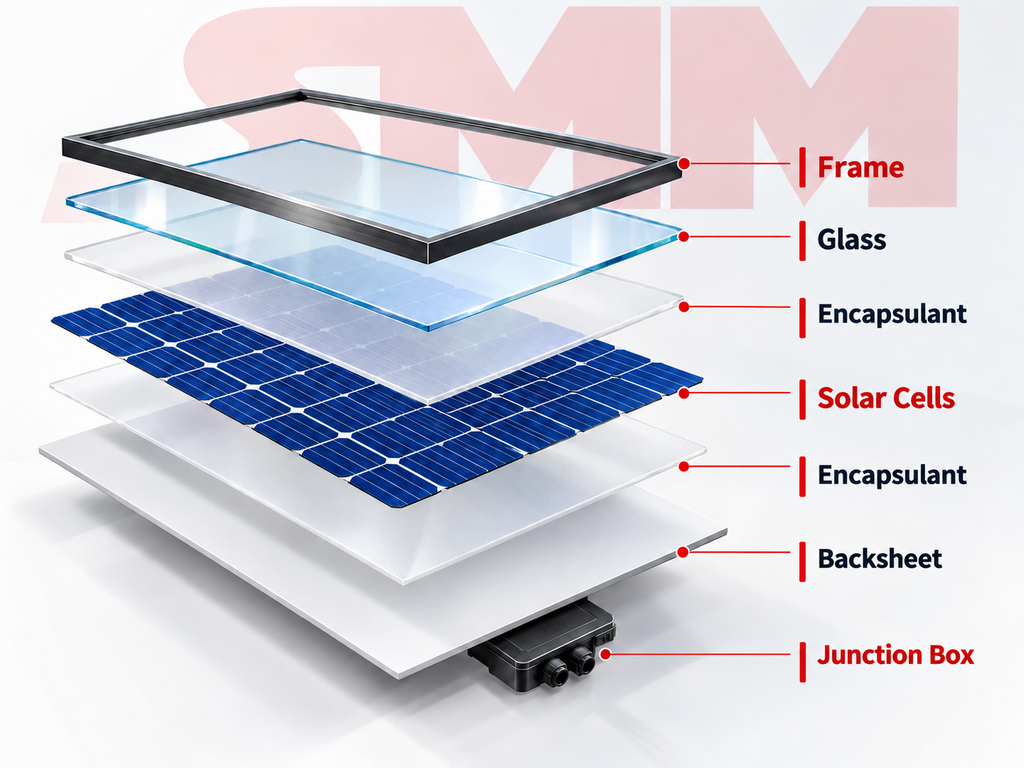
A conventional crystalline silicon PV module mainly consists of the following components:
| Component |
Main Function |
| Solar cells |
Convert sunlight into electricity |
| PV glass |
Allow light transmission and protect internal solar cells |
| Encapsulation films |
Bond, encapsulate, and protect solar cells |
| Backsheet / Rear glass |
Provide rear-side protection, electrical insulation, and weather resistance |
| Interconnection ribbons |
Connect solar cells and transmit electrical current |
| Aluminum frame |
Provide structural support and facilitate transportation and installation |
| Junction box and cables |
Transfer electricity generated inside the module to external systems |
Common encapsulation films include EVA, POE, and other materials.
These films surround the solar cells and provide bonding, cushioning, and environmental protection during the encapsulation process.
Depending on the rear-side encapsulation structure, the market also includes single-glass and double-glass modules.
Conventional single-glass modules typically feature front glass and a backsheet, while double-glass modules use rear glass instead of a traditional backsheet.
Interconnection ribbons connect individual solar cells and transmit electrical current through the module's internal circuitry.
The junction box, typically installed on the rear side of the module, serves as an important interface between the module's internal electrical circuit and the external PV system. It also commonly contains bypass diodes and other electrical components.
A PV module is therefore not simply an enlarged solar cell. Instead, it is a complete product consisting of:
Electricity-Generating Units + Electrical Interconnections + Encapsulation Materials + Structural Components + Electrical Output Components
How Are These Materials Assembled into a PV Module?
After understanding the basic structure of a PV module, the next step is to examine how these materials are assembled into a finished product.
Module manufacturing begins with establishing electrical connections between solar cells.
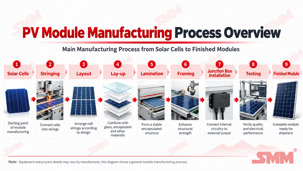
The cells are arranged according to the product design and interconnected using conductive ribbons to form cell strings. These strings are subsequently arranged and connected in accordance with the module's electrical configuration, gradually forming the internal circuit structure.
Once the electrical arrangement is completed, the cell strings are layered with glass, encapsulation films, and rear-side materials.
The assembled structure then enters the lamination process, during which controlled temperature, vacuum, and pressure conditions are applied to form a stable encapsulated structure.
Following lamination, the module undergoes additional manufacturing processes, including frame installation, junction box assembly, and cable connection.
After these stages, the module's basic structure and external appearance are largely complete.
The overall manufacturing process can be simplified as follows:
Solar Cells → Stringing and Soldering → Cell Layout → Layup → Lamination → Framing → Junction Box Installation → Testing → Finished PV Modules
However, module manufacturing does not end with physical assembly.
Finished modules must undergo appropriate quality, electrical performance, and safety tests.
Different production stages involve various inspection procedures, while specific quality control practices may differ among manufacturers. These testing procedures are therefore not discussed individually here.
Once the modules pass the required inspections, they proceed to power classification, packaging, and shipment before being supplied for integration into PV systems.
This manufacturing process demonstrates that module production involves considerably more than simply combining different materials.
Its core function is to:
- Establish stable electrical connections between individual electricity-generating units and integrate them into a protected structure capable of long-term operation.
Starting from quartz raw materials, the manufacturing process proceeds through metallurgical-grade silicon, polysilicon, silicon wafers, and solar cells before reaching the finished PV module.
The overall transformation can be summarized as:
Raw Material Purification → Semiconductor Material Processing → Photovoltaic Device Manufacturing → Electrical Interconnection and Encapsulation
At this stage, the fundamental questions of where a PV module comes from, what it consists of, and how it is manufactured have been addressed.
However, once modules enter the market, they are available in a wide variety of sizes, configurations, and product designs.
II. PV Module Specifications: Cell Formats, Cutting Methods, and Cell Dimensions
PV module specifications are not determined by a single parameter.
Product specifications commonly refer to 48-format, 54-format, 66-format, and 72-format modules, as well as configurations such as 108 half-cells, 132 half-cells, 18X, 210, and 210R.
These terms do not represent the same classification dimension. Instead, they describe different aspects of module design.
The module format primarily reflects the basic cell arrangement and full-cell-equivalent count. The cell cutting method describes how cells are divided and interconnected within the module. Cell dimensions indicate the size specifications of the silicon wafers and cells used.
Together, these factors influence the module's overall dimensions, weight, power output, electrical configuration, and suitability for different applications.
To understand module specifications, three concepts should therefore be distinguished:
- Module format — How are the cells arranged within the module?
- Cell cutting method — Are the cells used in full-cell, half-cell, or multi-cut configurations?
- Cell size category — What cell dimensions are used, such as 18X, 210, or 210R?
These factors must then be considered alongside module dimensions, weight, output power, and intended applications to establish a more complete understanding of a particular PV module.
What Is a PV Module Format?
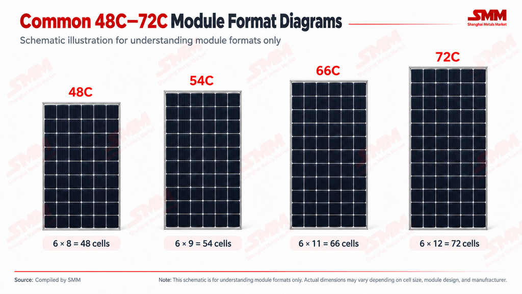
Common module formats include 48-format, 54-format, 66-format, and 72-format configurations.
From a product design perspective, the format is primarily associated with the full-cell-equivalent count and basic cell arrangement.However, its influence extends beyond the number of cells. It also affects module dimensions, weight, output power, handling and installation requirements, rooftop compatibility, and overall system design.The development of different module formats essentially reflects the efforts of manufacturers to balance module size, individual module power, and project suitability across different applications.
Smaller formats, such as 48-format and 54-format modules, generally allow manufacturers to maintain relatively manageable dimensions and weight.They are therefore commonly used in residential rooftop installations, small-scale distributed PV systems, and certain commercial and industrial (C&I) rooftop projects.In these applications, available roof space, manual handling, installation convenience, and compatibility with other system equipment are important design considerations.
By comparison, 66-format, 72-format, and larger modules can accommodate more cell units and more readily achieve higher power output per module.They are therefore more commonly used in large C&I installations and utility-scale PV projects.These applications typically place greater emphasis on the number of modules required per unit of installed capacity, mounting structures, electrical system configurations, balance-of-system (BOS) costs, transportation efficiency, and large-scale installation productivity.
The common applications and design considerations of different formats can be summarized as follows:
| Module Format |
Common Application Scenarios |
Main Product Design Considerations |
| Smaller formats, such as 48 / 54 |
Residential rooftops, small distributed PV systems, and certain C&I rooftops |
Module dimensions, weight, rooftop space utilization, handling, and installation convenience |
| Larger formats, such as 66 / 72 and above |
Large C&I projects and utility-scale ground-mounted PV installations |
Module quantity, BOS costs, transportation efficiency, and large-scale installation productivity |
It should be emphasized that there is no strict one-to-one relationship between module formats and application scenarios.
Module formats primarily describe the basic cell arrangement, while the actual dimensions, weight, and power output also depend on cell size, conversion efficiency, cutting method, and module structure.
As a result, products using the same format may serve different market segments depending on their specific designs.
For example, 54-format modules can be used in both residential and certain C&I applications, while 72-format modules, although more common in large C&I and utility-scale projects, are not restricted to a single application category.
Under otherwise comparable conditions, smaller formats generally offer advantages in controlling module size and weight, improving handling and installation flexibility.
Larger formats, meanwhile, can more readily achieve higher power output per module and reduce the number of modules required for a given installed capacity.
However, the suitability of a specific product must still be assessed based on transportation requirements, installation conditions, module weight, mounting structures, electrical system configuration, and overall BOS costs.
From Full Cells to Half-Cut and Multi-Cut Cells: How Does Cell Cutting Affect Module Design?
In addition to module formats, product specifications often include terms such as "108 half-cells," "132 half-cells," and "multi-cut cells."
These terms primarily refer to cell cutting methods and the module's internal electrical design.
Taking a 54-format module as an example, a conventional full-cell configuration has a full-cell-equivalent count of 54.
When each full-size cell is divided into two half-cells, the module contains 108 half-cell units:
54 Full-Size Cells → 108 Half-Cell Units
Therefore, "54-format" and "108 half-cells" do not represent two separate module categories.
The former describes the module format and full-cell-equivalent count, while the latter refers to the actual number of cell units after cutting.
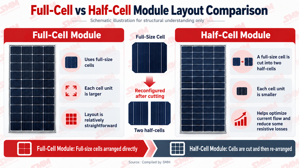
The primary purpose of half-cut cell technology is not simply to increase the number of cell units inside a module.Instead, it is to optimize electrical current transmission and the internal circuit configuration.When a full-size cell is divided into two half-cells, the operating current of each half-cell decreases accordingly.When combined with a redesigned series-parallel configuration, this can reduce resistive losses along certain interconnection paths.Because resistive power losses are proportional to the square of the current, reducing current helps lower these losses and improve module output performance.
The main benefits of half-cut cell configurations therefore include:
- Reducing resistive losses along certain interconnection paths;
- Optimizing current transmission within the module;
- Providing greater flexibility in series-parallel circuit design;
- Improving module output performance under certain conditions.
Building on half-cut cell designs, some modules further divide full-size cells into a greater number of smaller units, commonly referred to as multi-cut cell configurations.
The underlying principle is similar to that of half-cut technology: adjusting individual cell dimensions, operating current, and interconnection methods to optimize the module's internal electrical structure.
From a product design perspective, the progression can be understood as:
Full Cells → Half-Cut Cells → Multi-Cut Cells
As the degree of cell cutting increases, individual cell units become smaller, potentially providing greater flexibility in module layout and electrical interconnection.However, increasing the number of cell segments does not automatically produce a better module.More complex cutting methods also place greater demands on cutting quality, interconnection processes, equipment compatibility, manufacturing costs, and long-term reliability.Therefore, full-cell, half-cut, and multi-cut designs should not be viewed as a simple progression in which more cell segments necessarily indicate more advanced technology.
Instead, manufacturers must balance:
- Electrical performance;
- Manufacturing processes;
- Cost and reliability.
How Do Cell Dimensions Affect Module Specifications?
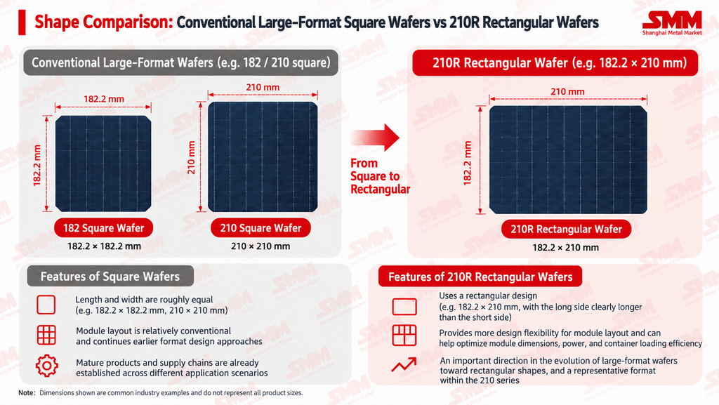
Beyond module formats and cell cutting methods, cell dimensions are another important factor influencing PV module specifications. There is no fixed one-to-one relationship between module formats and cell dimensions. In practice, different cell size categories may be applied to different module formats, while modules using the same format may incorporate different cell dimensions. Consequently, the dimensions of cells used in a module cannot be determined solely from its format. Specific product parameters must also be considered. Historically, the industry commonly distinguished between 182 mm and 210 mm silicon wafer and solar cell size categories. However, with the development of rectangular silicon wafers, cell dimensions are no longer limited to conventional square specifications. Within the 182 mm size category, the market has gradually introduced specifications such as 182.2 × 183.x mm and 182.2 × 191.x mm, resulting in increasingly diverse dimensional combinations.
In certain industry product classifications and market statistics, products developed around the 182 mm size category are commonly grouped under the term:
It is important to note that 18X does not represent one fixed dimension. Instead, it is a generalized industry term used to describe a range of silicon wafer and solar cell specifications developed from the 182 mm size category. Its precise dimensional coverage may vary between manufacturers and statistical methodologies. Meanwhile, the 210 mm size category has also evolved from traditional square wafers toward rectangular designs.
One commonly referenced category is:
The letter "R" generally stands for Rectangular. Compared with conventional square wafers measuring approximately 210 × 210 mm, 210R emphasizes rectangular dimensions, including specifications such as 182.2 × 210 mm available in the market.
The development of rectangular cell dimensions provides manufacturers with additional flexibility when balancing:
- Module length and width;
- Individual module power output;
- Shipping container loading efficiency;
- Manual handling;
- Installation requirements.
The final selection of module format, cell dimensions, and cutting method is not determined by any single factor. Instead, it reflects the combined influence of cell specifications, module design, manufacturing processes, and downstream application requirements. The module format establishes the basic cell arrangement, cell dimensions influence the module's physical size and achievable power output, and the cutting method further affects internal electrical connections and current pathways. Therefore, understanding a PV module requires considering its format, cell dimensions, cutting method, overall dimensions and power output, and intended application. Terms such as 48-format, 108 half-cells, 18X, and 210R are not independent concepts. Rather, they describe different dimensions of PV module design.
III. What Are the Main Types of PV Module Technologies?
The global PV module market is currently dominated by crystalline silicon technology. At the same time, thin-film PV technologies such as cadmium telluride (CdTe), copper indium gallium selenide (CIGS), and amorphous silicon have achieved commercial applications. Emerging technologies, including perovskite solar cells and perovskite/silicon tandem cells, are also progressing through research, development, and industrialization. Crystalline silicon modules use silicon wafers and crystalline silicon solar cells as their core components and currently represent the dominant technology category in the PV market. Within crystalline silicon solar cell technology, several different technology pathways and structural designs can be identified, including BSF, PERC, TOPCon, HJT, and BC.
In addition to differences in cell structures and manufacturing processes, these technologies also involve a fundamental classification:
- P-type solar cells
- N-type solar cells
More specifically:
- BSF is an earlier crystalline silicon cell technology that historically relied primarily on P-type designs.
- PERC was the dominant market technology for many years, with P-type PERC being the most common configuration.
- TOPCon has become one of the mainstream N-type cell technology pathways.
- HJT also primarily uses N-type silicon wafers and represents another high-efficiency N-type technology pathway.
- BC primarily refers to a back-contact cell structure. Current commercial high-efficiency BC products predominantly use N-type silicon wafers.
The main technologies can be summarized as follows:
| Technology |
Common Type |
Basic Description |
| BSF |
Primarily P-type |
Earlier-generation crystalline silicon cell technology |
| PERC |
Primarily P-type |
Previously dominant solar cell technology |
| TOPCon |
Primarily N-type |
One of the mainstream N-type cell technologies |
| HJT |
Primarily N-type |
High-efficiency N-type heterojunction technology |
| BC |
Primarily N-type |
Primarily refers to a back-contact cell structure |
In simple terms, P-type and N-type mainly describe the conductivity type of the silicon substrate.
PERC, TOPCon, and HJT refer primarily to different cell structures and manufacturing technology pathways, while BC mainly describes a back-contact structure.
Consequently, product specifications and technical documentation commonly use combinations such as:
- P-type PERC
- N-type TOPCon
- N-type HJT
Why Has TOPCon Rapidly Become a Mainstream Technology?
In recent years, crystalline silicon solar cell technology has been transitioning from conventional P-type PERC toward higher-efficiency N-type technologies. Among these, TOPCon has become one of the mainstream N-type technology pathways. On the one hand, N-type silicon wafers offer certain advantages in material properties, degradation characteristics, and potential efficiency improvements. On the other hand, TOPCon uses tunnel oxide layers and passivated contact structures to reduce certain carrier recombination losses, thereby improving cell conversion efficiency.
Compared with conventional P-type PERC, N-type TOPCon generally offers:
- Higher front-side conversion efficiency, allowing its efficiency advantages to be reflected even in monofacial modules;
- A relatively high bifaciality factor when used in bifacial module designs;
- Further potential for conversion efficiency improvements;
- Lower sensitivity to certain degradation mechanisms commonly associated with conventional P-type PERC;
- Good process compatibility with existing crystalline silicon manufacturing infrastructure, supporting large-scale industrialization.
It is worth noting that TOPCon's advantages are not limited to bifacial power generation.
Even when incorporated into monofacial modules, its higher front-side conversion efficiency can provide performance benefits.
In bifacial module configurations, a higher bifaciality factor can further improve the utilization of sunlight reaching the rear side of the module.
Therefore, TOPCon's rapid commercialization has not resulted solely from the higher efficiency associated with N-type technology.
Rather, it reflects a favorable balance among:
- Conversion efficiency, manufacturing costs, process compatibility, and industrial maturity.
Beyond Cell Technology: What Other Interconnection Methods Are Used in PV Modules?
In addition to cell technology pathways and structural designs such as PERC, TOPCon, HJT, and BC, PV modules can also adopt different cell interconnection and arrangement methods.
One representative technology is:
Shingled modules typically divide full-size solar cells into relatively narrow strips, which are then arranged and electrically connected through an overlapping configuration. Compared with conventional half-cut or multi-cut cell designs, the defining feature of shingled technology is not simply the further reduction of cell dimensions. It also changes the arrangement and interconnection structure between individual cell units. This design can reduce the gaps between conventional cell units and certain interconnection-related shading losses, increase the effective light-receiving area and packing density of the module, and redesign internal current transmission pathways. Therefore, shingled technology is more appropriately understood as a module interconnection technology, rather than simply another cell cutting method.
Thin-Film Photovoltaics
Unlike crystalline silicon PV modules, thin-film photovoltaic technologies do not rely on conventional crystalline silicon wafers as their core material. Instead, they generally involve depositing thin layers of semiconductor materials onto substrates such as glass, metal, or other suitable materials to achieve photovoltaic conversion.
Common thin-film technologies include:
- CdTe (Cadmium Telluride)
- CIGS (Copper Indium Gallium Selenide)
- Amorphous Silicon Thin-Film Technology, among others.
Compared with crystalline silicon modules, thin-film products differ in material systems, manufacturing processes, temperature characteristics, and application scenarios.However, crystalline silicon modules continue to dominate the overall PV market in terms of market scale. Thin-film and crystalline silicon technologies should not be viewed simply as direct substitutes. Instead, they represent different photovoltaic technology pathways based on distinct materials and manufacturing processes.
Perovskite Photovoltaics
In addition to commercially established crystalline silicon and thin-film technologies, the PV industry continues to develop new technology pathways.
One area attracting considerable attention is:
Perovskite photovoltaics represent an emerging generation of solar cell technology and remain in a period of rapid research, development, and industrialization.
Current development directions include:
- Single-Junction Perovskite Solar Cells
Perovskite solar cells use semiconductor materials with a perovskite crystal structure to absorb sunlight and convert it into electricity.These materials offer considerable potential for high conversion efficiency.At present, perovskite photovoltaics are therefore more appropriately regarded as an emerging technology progressing toward broader commercialization, rather than an established mainstream technology that has already replaced crystalline silicon modules.
The broader PV technology landscape can be summarized as follows:
| Technology Category |
Representative Technologies |
Current Development Status |
| Crystalline Silicon PV |
BSF, PERC, TOPCon, HJT, BC |
Dominant technology category in the current market |
| Thin-Film PV |
CdTe, CIGS, etc. |
Commercialized, but accounts for a relatively small share of the overall market |
| Emerging PV Technologies |
Perovskite, Perovskite/Silicon Tandem |
Continuing research, development, and industrialization |
Overall, the PV module market remains dominated by crystalline silicon technology, while crystalline silicon solar cells are transitioning from conventional P-type PERC toward higher-efficiency N-type technologies.Among these, TOPCon has become one of the mainstream technology pathways, while HJT and various BC technology configurations continue to develop.Thin-film photovoltaics and perovskite technologies, meanwhile, represent different directions in the broader evolution of solar cell technologies.
From a supply chain perspective, PV modules connect upstream silicon materials and solar cell manufacturing with downstream PV systems, serving as a key stage in transforming photovoltaic devices into finished products.The progression from quartz, metallurgical-grade silicon, and polysilicon to silicon wafers and solar cells, followed by electrical interconnection, encapsulation, and structural assembly, reflects an integrated sequence of material processing, semiconductor manufacturing, and module design.At the module product level, cell formats, dimensions, cutting methods, and cell technologies further distinguish different product configurations.
Industry terms such as 48-format, 18X, 210R, TOPCon, HJT, and BC describe different aspects of product specifications, dimensional categories, and technology pathways. Together, they define the main technical and structural characteristics of PV modules.Understanding PV modules can therefore begin with several fundamental questions:
Where do PV modules come from? What are they made of? How are their specifications designed? And which solar cell technologies do they use?
Within this framework, polysilicon, silicon wafers, solar cells, module formats, cell dimensions, and technology pathways are not isolated concepts. Instead, they represent interconnected aspects of a complete PV module product. As solar cell technologies, material systems, and downstream market requirements continue to evolve, PV modules will undergo further optimization in conversion efficiency, power output, reliability, cost, and compatibility with different PV system applications.


![[SMM PV Flash] Environmental Assessment Publicity for Gokin Solar PV Module Technological Transformation](https://imgqn.smm.cn/usercenter/GHTIQ20251217171741.jpg)
![[SMM PV Flash] PV-grade EVA Rally Continues](https://imgqn.smm.cn/usercenter/HdPjk20251217171741.jpg)
![[SMM PV News] AIKO ABC module achieves new breakthrough in the South African market, securing a 773.5 MW order](https://imgqn.smm.cn/usercenter/FmBvY20251217171737.jpg)