I. AI Computing Expansion — Unlocking a Second Growth Curve for Tin
The massive global rollout of AI infrastructure and data centers has quietly brought tin into the spotlight as the essential "Computational Solder." "Tin's low melting point (232°C), excellent electrical conductivity, and reliable joint strength make it an irreplaceable baseline material for electronic interconnects.
Currently, about 53% of global refined tin is used for solders, with electronics accounting for 70% of that share. This directly covers core AI hardware components, including server chip packaging, high-speed optical modules, and PCB board-level interconnections.
According to SMM, every GW of installed AI data center capacity requires approximately 1,200 to 1,500 tons of tin. The breakdown is roughly:
· Servers/GPUs/Networking: 500–1,500 tons
· Power and Switchgear: 100–400 tons
· Control/Comms/Cooling: 50–200 tons
Global AI computing installations are projected to grow at a 24% CAGR from 2025 to 2030, with a significant 65% year-over-year jump expected in 2026. The explosive demand for tin stems from a massive gap in usage between AI servers and traditional servers.
Driven by massive capital expenditure from US and Chinese cloud giants (AWS, Azure, GCP, Alibaba, Tencent, ByteDance), global AI server shipments are projected to hit 2.13 million units in 2025 and exceed 4 million by 2026. Consequently, data indicate that AI sectors now drive 60–70% of the growth in global tin consumption (including servers, AI PCs, optical modules, advanced packaging etc.), cementing its status as a core computational metal.
Data Source: SMM
II. Unit Tin Consumption in Computing Scenarios — Volatile Upward Trend and Long-Term Plateau
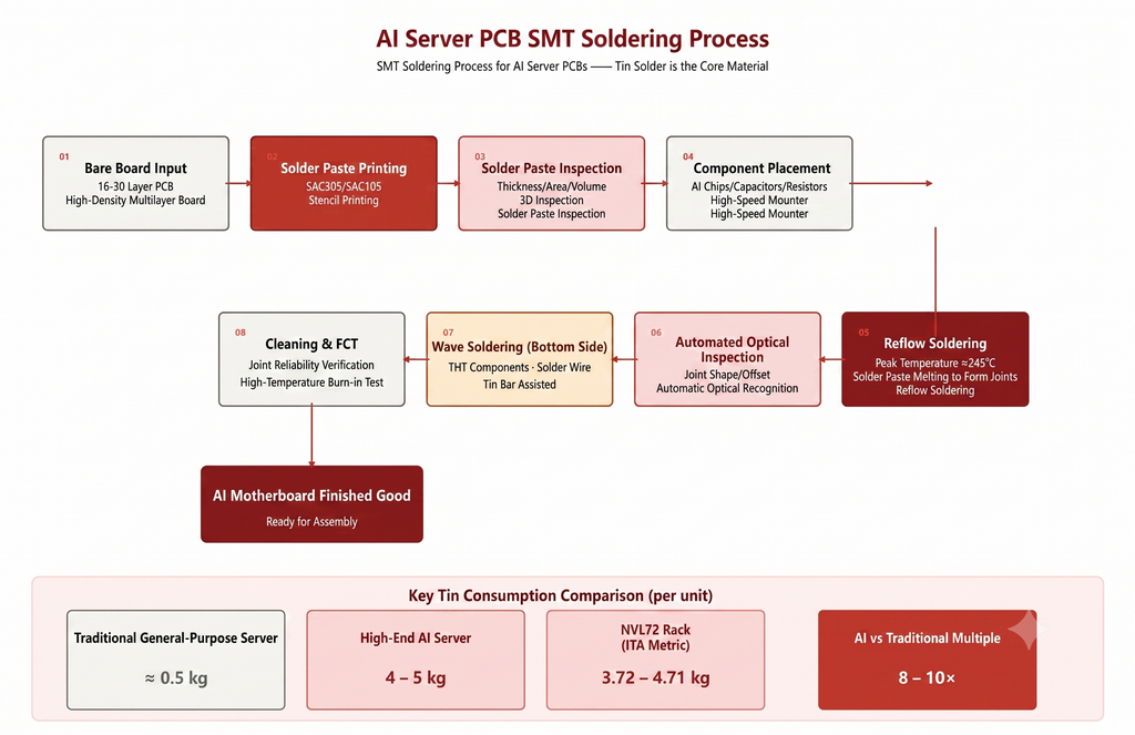
Understanding the demand resilience of tin in computing scenarios requires clarifying a key premise: Over 90% of tin in computing applications exists as solder, primarily lead-free systems such as tin-silver-copper alloys SAC305 and SAC105.
This metric dictates two core logics.
First, in the board-level soldering process, there is no mature path for aluminum materials or optical interconnect technologies to directly replace tin-based solder. The physical and chemical properties of tin, including a low melting point, high conductivity, and reliable wettability, possess structural rigidity in electronic soldering scenarios.
Second, in the short to medium term, HBM stacking increases solder joint density. Even if hybrid bonding scales up in certain advanced packaging after 2030, it will only form localized substitution.
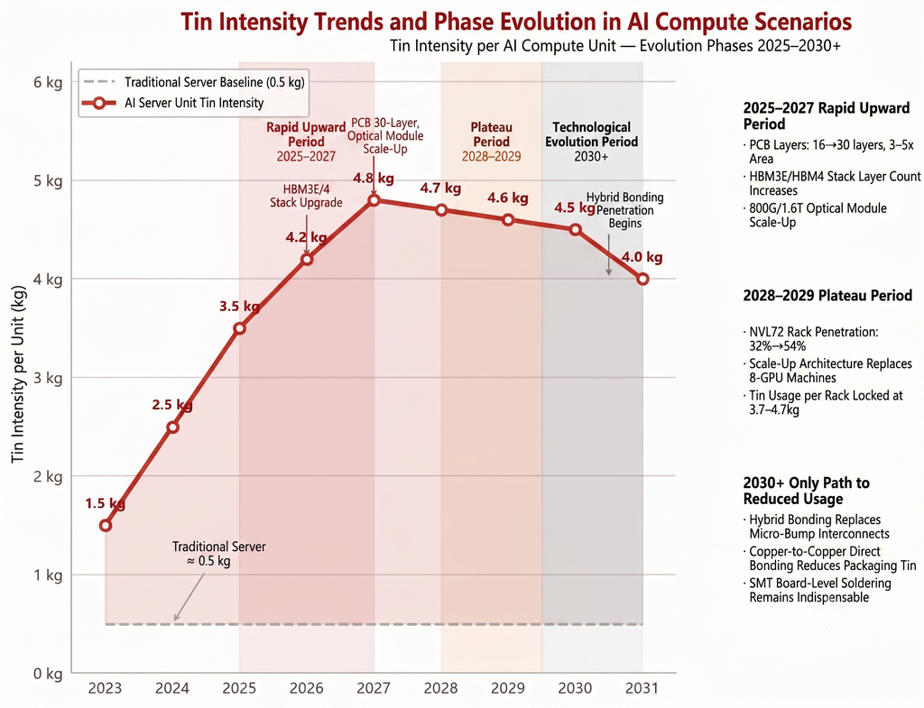
Overall, the unit tin consumption curve presents a pattern of a volatile upward trend followed by a long-term plateau:
Data Source: SMM
→ 2025 to 2027: Rapid Upward Phase in Unit Consumption
The current phase features a steep increase in unit tin consumption for AI servers. Three parallel technological drivers are overlapping during this period.
- Jump in PCB Layer Count and Area: AI server motherboard layer counts have increased from the traditional 8 to 12 layers up to 16 to 20 layers, and sometimes 30 layers. The PCB area has reached 3 to 5 times that of traditional machines. Multilayer boards result in a geometric increase in solder joints. Based on high-end AI server motherboard configurations, the incremental tin usage related to PCBs for a single AI server can reach up to approximately 1.32 kg.
- Generational Upgrades in HBM Stacking: As HBM3E advances to HBM4, the stacking layer count evolves from 8Hi to 12Hi and 16Hi. The number of micro-bumps between a single GPU and HBM reaches the hundreds of thousands, with spacing narrowing to 10 to 15 μm. The usage of BGA solder balls increases multiplicatively with I/O density. Each additional HBM stacking layer adds thousands to tens of thousands of micro-bumps, and every connection consumes tin-based solder.
- Leaps in Optical Module Speeds: 800G and 1.6T optical modules are entering a period of scaled production. The internal pad spacing of high-speed optical devices is only tens of micrometers, requiring specialized solder paste made from Type 4 to Type 8 ultra-fine tin powder. Although the tin consumption of a single optical module is small, in a 10,000-card intelligent computing center, optical modules are counted in the tens of thousands, providing clear elasticity in total volume.
→ 2028 to 2029: Unit Consumption Enters a Plateau
During this period, the growth of tin consumption will be driven more by the scale of installation volumes.
Post-2028, the upward momentum of unit tin consumption is expected to weaken marginally. The penetration rate of integrated AI rack architectures, such as NVL72 and GB200, is projected to rise from approximately 32.5% in 2026 to about 53.8% in 2030.
After Scale-Up architectures replace a portion of traditional 8-GPU servers, the tin consumption per rack is expected to stabilize roughly in the 3.7 to 4.7 kg range, lacking clear upward catalysts. In advanced packaging, Chiplet and 2.5D/3D CoWoS continue to penetrate, but tin usage for single-chip micro-bumps is already approaching the tens of grams level, slowing the marginal increment.
→ Post-2030: The Primary Downward Risk Path is Hybrid Bonding
In current technological roadmaps, Hybrid Bonding technology poses a potential downward risk to tin consumption. This technology removes tin-silver solder caps and adopts direct copper-to-copper bonding, theoretically reducing a portion of tin usage in the packaging process. However, its actual impact requires objective assessment.
Hybrid bonding is currently applied only in the most advanced process nodes, such as the back-end of HBM4+ and CIS image sensors. Scaled production is expected after 2030, and the penetration speed depends on yield improvements and cost convergence.
The key constraint is that board-level SMT soldering, which accounts for approximately 97% of total AI supply chain tin usage, currently cannot be replaced by hybrid bonding. Board-level soldering involves the electrical connection of thousands of components across the entire board, relying heavily on reflow soldering with solder paste and wave soldering with solder wire. These processes do not yet have a direct copper-to-copper replacement route.
Therefore, even if hybrid bonding gradually penetrates the advanced packaging sector, its impact on total tin consumption will be largely confined to the chip packaging stage, accounting for roughly 5% to 12%, rather than causing a systemic demand shock. Data source for these projections is SMM.
III. Tin Material Categories and Supply Chain Validation
Data Source: SMM
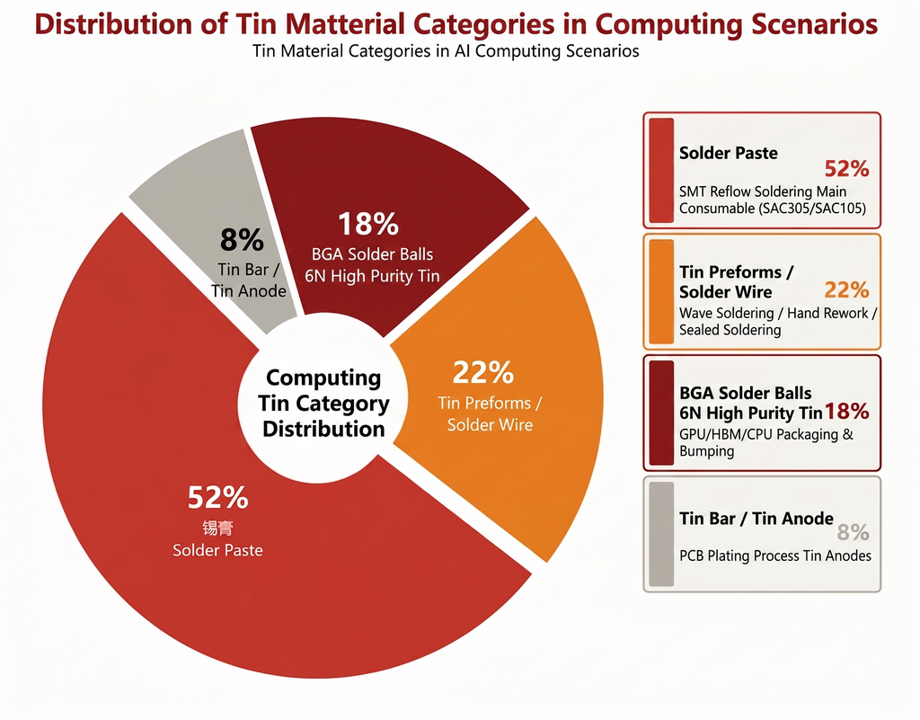
Based on SMM data, the market is divided into the following categories:
1. Solder Paste: Approximately 50% to 55%
Solder paste is the main consumable for SMT. Both AI server motherboards and optical module PCBs use solder paste reflow soldering as the core process. High-end categories are SAC305 (Sn96.5/Ag3.0/Cu0.5) and SAC105, which comply with RoHS lead-free requirements.
Ultra-fine powder specifications, from Type 4 to Type 8, are used for microscopic optical module pads. This is currently the specification with the tightest production capacity, reflecting new requirements for tin powder processing precision driven by computing upgrades.
2. Preformed Solder Preforms and Solder Wire: Approximately 20% to 25%
These are used in processes like wave soldering, manual rework, and optical module shell sealing. The consumption per rack is not large, but the total volume grows linearly with installation scale. This is a volume-driven category with relatively moderate price elasticity.
3. BGA Solder Balls (6N High-Purity Tin): Approximately 15% to 20%
This is the core consumable for GPU, HBM, and CPU packaging ball placement, holding the highest unit price among all tin material categories. The number of BGA solder balls on a single high-end AI chip ranges from thousands to tens of thousands. The supply landscape for 6N high-purity tin is highly concentrated. Tin Industry Shares holds the largest global market share, with Malaysia Smelting Corporation and Yunnan Chengfeng serving as primary supplementary suppliers.
The growth of this category benefits from both the increase in AI chip shipment volumes and the continuous rise in single-chip solder ball density caused by HBM stacking increasing I/O density. This classifies it as a category with simultaneous growth in volume and price.
4. Tin Bars and Tin Anodes: Approximately 5% to 10%
Tin anodes are used in the PCB electroplating process. The tin consumption for electroplating increases with high-layer-count AI server boards. Compared to other categories, the technical barriers and added value of tin anodes are low, making it a follower-growth category.
IV. Breakdown of Core Tin Usage in Computing Centers
Tin consumption in computing centers is concentrated in several clear segments. PCB board-level soldering is the absolute primary driver. Advanced packaging offers the highest growth elasticity despite its limited total volume proportion. Tin usage in power supply and distribution is extremely limited. The details are as follows.
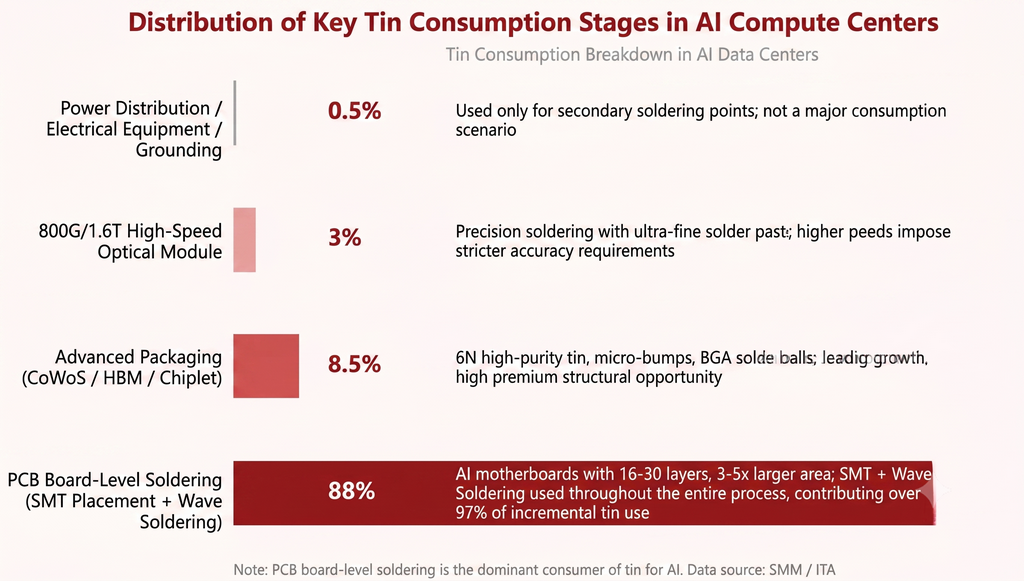
PCB Board-Level Soldering: 85% to 92%
All components on AI server motherboards, which have 16 to 30 layers and 3 to 5 times the area of traditional machines, are electrically connected via SMT and wave soldering. From GPU chips to surface-mount capacitors and resistors, this process relies entirely on tin-based solder, primarily paste and secondarily wire.
Within the incremental tin usage for AI, PCB electroplating and SMT contribute over 97%, acting as the true carrier of tin demand. For example, a 10,000-card AI computing center requires 2.5 to 3.2 tons of PCB solder alone. This indicates that tin consumption during the data center construction cycle features highly concentrated release characteristics.
Advanced Packaging (CoWoS/HBM/Chiplet): 5% to 12%
Processes such as GPU die-to-substrate bonding, HBM stacking and interposer interconnection, and micro-bumps between Chiplet dies widely use solder balls, micro-bumps, and ultra-fine solder paste made from 6N high-purity tin, which has a 99.9999% purity. The packaging tin usage for a single high-end AI chip can reach tens of grams, and the premium for 6N high-purity tin is significantly higher than that of standard tin ingots.
Statistics show that the chip segment, including advanced packaging and EUV lithography, accounts for only 2% to 3% of the total AI supply chain tin consumption. However, its leading growth rate and high unit price present a structural opportunity for the tin industry. Currently, major suppliers of 6N high-purity tin include Tin Industry Shares, Malaysia Smelting Corporation (MSC), and Yunnan Chengfeng, reflecting a highly concentrated supply landscape.
800G and 1.6T High-Speed Optical Modules: 2% to 5%
The interconnection of optical chips, lasers, and detectors with optical module substrates requires ultra-micro solder paste to achieve micrometer-level precision soldering. Optical module shell sealing and conductive soldering for high-speed connectors also use tin-based solder preforms.
The upgrade from 800G to 1.6T means pad spacing shrinks further, ensuring continued demand growth for ultra-fine tin powder specifications of Type 6 and above.
Power Supply, Distribution, and Grounding: Under 1%
Only the auxiliary solder joints in data center low-voltage distribution cabinets, UPS systems, and grounding copper grids use a small amount of solder. This does not constitute a main consumption scenario for tin. The proportion of the power distribution segment in total tin consumption is small. Tin's role in the computing chain is essentially connection rather than transmission, making the solder joint the true carrier of tin.
V. Conclusions
First, the pull of AI computing expansion on tin consumption is structural rather than cyclical. Traditional servers consume about 0.5 kg of tin per unit, whereas AI servers have reached 4 to 5 kg. This 8 to 10-fold jump is a reconstruction of the demand function rather than a gradual upgrade. SMM forecasts a 24% CAGR for global newly installed computing capacity from 2025 to 2030. This growth rate, combined with the continuous rise in per-unit consumption, indicates that tin's consumption elasticity in the AI computing chain will be noticeably higher than that of most industrial metals.
Second, PCB board-level soldering is the absolute primary demand source for tin in AI computing. PCB board-level soldering accounts for 85% to 92% of AI tin usage. From an incremental perspective, PCB electroplating and SMT placement contribute over 97%. A 10,000-card AI computing center requires 2.5 to 3.2 tons of PCB solder alone, while the power supply and distribution segment accounts for less than 1%. Tin's role in the computing chain is essentially connection rather than transmission. Solder is the fundamental identity of tin and the root source of its demand resilience.
Third, the unit tin consumption curve moves upward in the short term, plateaus in the medium term, and faces structural substitution risks in the long term, though the substitution scope is limited. The years 2025 to 2027 represent a rapid upward phase for unit consumption, driven by increased PCB layers, HBM stacking, and optical module speeds. The years 2028 to 2029 enter a plateau phase as Scale-Up architectures lock in per-rack tin usage. Post-2030, hybrid bonding may form localized substitution in the advanced packaging segment, which accounts for 5% to 12% of AI tin usage. However, board-level SMT soldering, holding the absolute majority share at roughly 97%, has no substitution path.
Finally, there is distinct divergence among tin material categories. Solder paste, accounting for 50% to 55%, benefits from PCB area expansion and layer count increases, categorizing it as a volume-driven product. BGA high-purity solder balls, accounting for 15% to 20%, benefit from increased chip packaging density and the 6N premium, classifying it as a volume-and-price growth product. Preformed solder preforms and tin anodes are follower-growth categories. Within the AI computing investment cycle, solder paste and BGA solder balls are the categories with the highest elasticity.
Overall, tin's position within the computing metal narrative is systematically undervalued by the market. While the hardware demand for computing infrastructure has been fully priced in, tin serves as the computational solder. From server motherboards to chip packaging and optical module interconnections, it covers the interconnection needs of nearly every key link in AI hardware. The re-evaluation of its value has just begun.

![Bullish and bearish factors intertwined to cause disruptions, and the most-traded SHFE tin contract saw wild swings intraday [SMM Tin Brief]](https://imgqn.smm.cn/usercenter/qWcEp20251217171751.jpeg)